(China (Mainland))

Product Summary
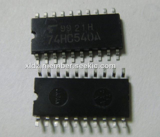
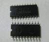
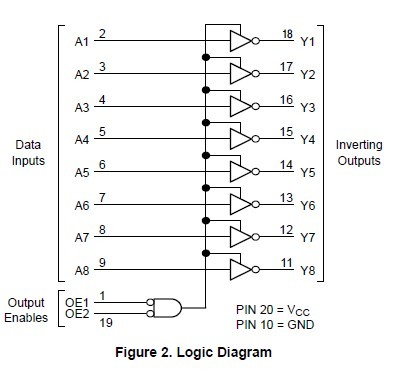
The 74HC540A is an octal inverting buffer/line driver/line receiver designed to be used with 3-state memory address drivers, clock drivers, and other bus-oriented systems. The 74HC540A is identical in pinout to the LS540. The device inputs are compatible with Standard CMOS outputs. External pull-up resistors make them compatible with LSTTL outputs. This device features inputs and outputs on opposite sides of the package and two ANDed active.low output enables.
Parametrics
74HC540A absolute maximum ratings: (1)VCC, DC Supply Voltage: -0.5 to +7.0 V; (2)VI, DC Input Voltage: -0.5 to VCC +0.5 V; (3)VO, DC Output Voltag: -0.5 ≤ VO ≤ VCC +0.5 V; (4)IIK, DC Input Diode Current: ±20 mA; (5)IOK, DC Output Diode Current: ±35 mA; (6)IO, DC Output Sink Current: ±35 mA; (7)ICC, DC Supply Current per Supply Pin: ±75 mA; (8)IGND, DC Ground Current per Ground Pin: ±75 mA; (9)TSTG, Storage Temperature Range: -65 to +150℃; (10)TL, Lead Temperature, 1 mm from Case for 10 Seconds 260℃; (11)TJ, Junction Temperature Under Bias: +150℃; (12)θJA, Thermal Resistance, PDIP: 67℃/W; SOIC: 96℃/W; TSSOP: 128℃/W; (13)PD, Power Dissipation in Still Air at 85℃, PDIP: 750mW; SOIC: 500mW; TSSOP: 450 mW.
Features
74HC540A features: (1)Output Drive Capability: 15 LSTTL Loads; (2)Outputs Directly Interface to CMOS, NMOS, and TTL; (3)Operating Voltage Range: 2.0 to 6.0 V; (4)Low Input Current: 1 μA; (5)High Noise Immunity Characteristic of CMOS Devices; (6)In Compliance With the JEDEC Standard No. 7A Requirements; (7)Chip Complexity: 124 FETs or 31 Equivalent Gates; (8)Pb-Free Packages are Available.
Diagrams
 |
 74HC |
Other |
|
Data Sheet |
Negotiable |
|
||||
|
74HC/HCT02 |
Other |
|
Data Sheet |
Negotiable |
|
||||
|
74HC/HCT03 |
Other |
|
Data Sheet |
Negotiable |
|
||||
|
74HC/HCT10 |
Other |
|
Data Sheet |
Negotiable |
|
||||
|
74HC/HCT107 |
Other |
|
Data Sheet |
Negotiable |
|
||||
|
74HC/HCT109 |
Other |
|
Data Sheet |
Negotiable |
|
||||