Product Summary
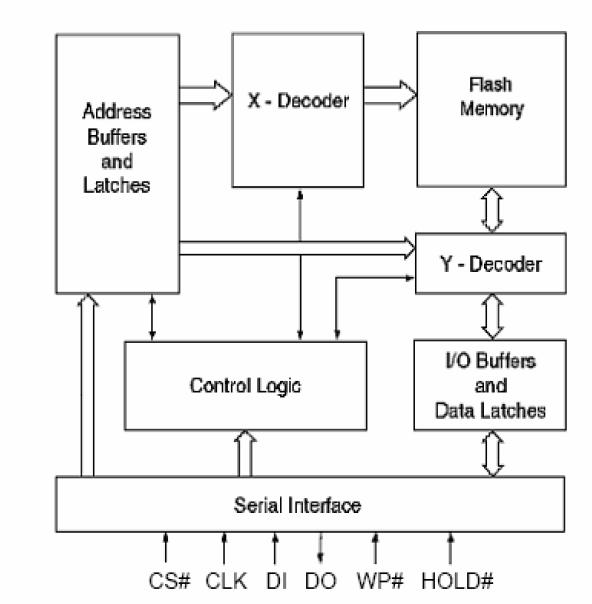
The EN25F80-100 is an 8M-bit (1024K-byte) Serial Flash memory, with advanced write protection mechanisms, accessed by a high speed SPI-compatible bus. The memory can be programmed 1 to 256 bytes at a time, using the Page Program instruction. The EN25F80-100 is designed to allow either single Sector at a time or full chip erase operation. The EN25F80-100 can be configured to protect part of the memory as the software protected mode. The device can sustain a minimum of 100K program/erase cycles on each sector.
Parametrics
EN25F80-100 absolute maximum ratings: (1)Storage Temperature: -65 to +125℃; (2)Plastic Packages: -65 to +125℃; (3)Output Short Circuit Current: 200 mA; (4)Input and Output Voltage (with respect to ground): -0.5 to +4.0 V; (5)Vcc: -0.5 to +4.0 V.
Features
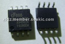
EN25F80-100 features: (1)Single power supply operation, Full voltage range: 2.7-3.6 volt; (2)8 Mbit Serial Flash, 8 M-bit/1024 K-byte/4096 pages; 256 bytes per programmable page; (3)High performance, 100MHz clock rate; (4)Low power consumption, 5 mA typical active current; 1μA typical power down current; (5)Uniform Sector Architecture: 256 sectors of 4-Kbyte; 16 blocks of 64-Kbyte; Any sector or block can be erased individually; (6)Software and Hardware Write Protection; (7)High performance program/erase speed; (8)Lockable 256 byte OTP security sector; (9)Minimum 100K endurance cycle; (10)Package Options, 8 pins SOP 200mil body width; 8 contact VDFN; 8 pins PDIP; All Pb-free packages are RoHS compliant; (11)Commercial and industrial temperature Range.
Diagrams

 |
 EN25B32 |
 Other |
 |
 Data Sheet |
 Negotiable |
|
||||
 |
 EN25B40 |
 Other |
 |
 Data Sheet |
 Negotiable |
|
||||
 |
 EN25B64 |
 Other |
 |
 Data Sheet |
 Negotiable |
|
||||
 |
 EN25B80 |
 Other |
 |
 Data Sheet |
 Negotiable |
|
||||
 |
 EN25D16 |
 Other |
 |
 Data Sheet |
 Negotiable |
|
||||
 |
 EN25F05 |
 Other |
 |
 Data Sheet |
 Negotiable |
|
||||
 (China (Mainland))


